8-Way Switch

Our Team

Brian Padilla

EE Undergrad / Team Member

Brian Padilla is a 2nd year transfer who embodies what it means to  Learn by Doing. Whether it be in DIY projects, classwork, or in a professional setting he is always looking for opportunities to get his mind busy and hands dirty.

Elizaveta Koush

EE Undergrad / Team member

Elizaveta is a 3rd year student from Palo Alto. She is majoring in electrical engineering and minoring in economics. She loves to learn through projects, in which she gets the opportunity to build a deep understanding of many interdependent parts.

Abstract

In this project, we will work with project sponsors at Raytheon to design and fabricate a 1 by 8 solid state switch that covers the frequency range of 50 MHz to 18 GHz using surface mount components and low-loss dielectric substrates.    We will start by verifying models for p-i-n switch diodes using Keysight Advanced Design systems software.   We will then model the entire switch using a 2.5 dimension electromagnetic simulator to model the parasitic coupling between transmission lines for this star-configuration switch.   The last task will be to do the layout and ready design for fabrication.   If time permits we might be able to do a first pass fabrication of the design.

Acknowledgements

We are extremely appreciative of Raytheon, the Masters student, Andre Vigano, our faculty advisor, Dennis Derickson, and Raytheon Engineer, Shane O’Connor for the opportunity to participate in such an interesting project. Their input was extremely formative in the direction of the project as well as our experience.

Our/My Project Video (optional)

Project Overview

Transmission Line Transition by Via Hole

Description:

It is desirable to have the 8-Way Switch obtain the capability to be mounted onto a daughter board and carried off to the motherboard.

This transition achieved with transmission lines and vias. At high RF via holes act as inductors. In order to mitigate this and additional EM buildup in this layout to achieve low loss the following were optimized:

  • T-Line Design (Impedance Matching)
  • Geometric Tuning
  • Substrate Selection & Height
  • Ground Plane & Grounding Vias
 

Model Specifics:

  • The 3D Keysight ADS model above features a upper & lower substrate with a loosely bounded CPWG (red) & CPWG (blue). All vias adjacent to these T-Lines are grounding vias while the center half-via is for the main transition.  
  • With tapered CPWG spacing, grounding vias, a substrate Er = 3.66, and 50 Ohm optimized T-Lines the overall S(2,1) parameters below are produced with an overall max loss of -0.30dB at 18 GHz:

Thank you Raytheon sponsors!
This has been a tremendous learning experience and we are delighted that Cal Poly students were able to contribute to your future endeavors. We appreciate this opportunity and greatly value Cal Poly’s relationship with Raytheon.

8-Way Switch

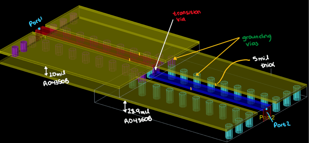
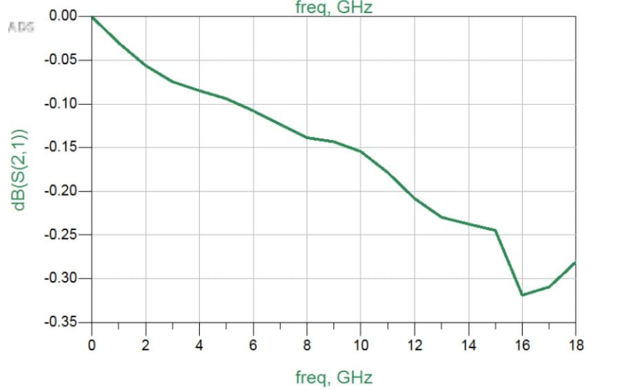
The aspects described conjoin to achieve the common goal of the SMT 8-Way Switch with a desired frequency range is 0.05 to 18 GHz. The modeling of the PIN Diode contributes to accurate testing of potential switch geometries while the Motherboard via transition allow the adjacent designs to function with other implemented SMT components. 

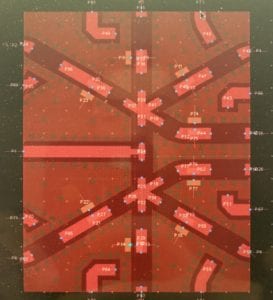
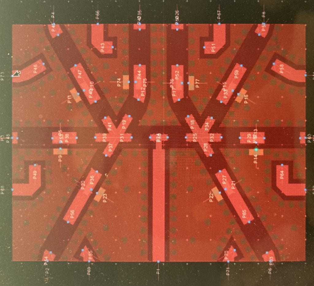
The image above displays the current draft of the 8 way switch design. This aspect is still in progress and will most likely change in the following months. This design was created by Andre Vigano as a part of his thesis.

PIN Diode Modeling

Progress Timeline:

  • Learn how to use ADS
  • Investigate potential model options
  • Test Vendor Models
  • Verify the ADS generic PIN Diode model
  • Develop a thorough PIN Diode model
  • Simulate the model to confirm its accuracy
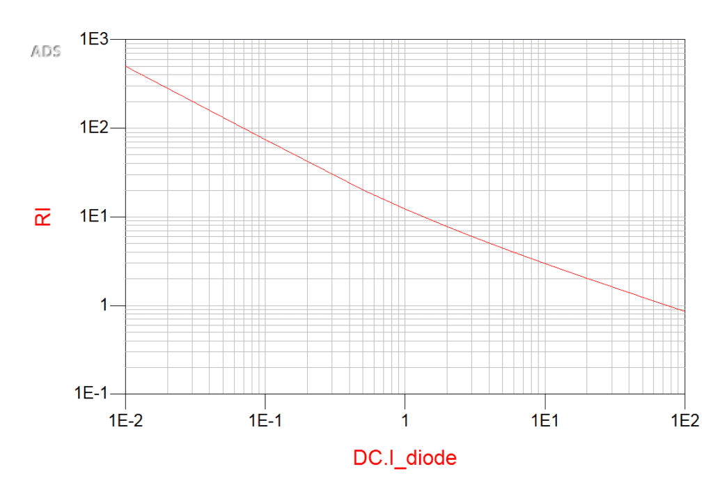
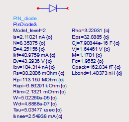
The Process

By adjusting and optimizing the diode parameters in ADS, an accurate PIN Diode model can be obtained. 

Comparing model properties to those specified on data sheets serves as a confirmation of their reliability. Data sheet information is compared to graphs obtained in ADS (see figure below) to ensure an accurate model. 

The final step entails simulating the given model to ensure that it is accurate over all parameter considerations.

Share

Share on facebook
Share on twitter
Share on linkedin

Coronavirus Update and Resources